
1. Introduction of precision dicing machine industry
A dicing machine is a device that uses a blade or a laser to cut the workpiece with high precision. It is the key equipment for wafer cutting and WLP cutting in the semiconductor back-end packaging and testing. With the development of integrated circuits in a large-scale direction, the dicing process has shown a trend of becoming more refined and efficient. From the scribing method that relies on manual operation in the 1860s, the diamond grinding wheel scribing machine invented by the British LP Company in 1968 replaced the traditional scribing and breaking process with the grinding process. The automatic dicing machine further improves the efficiency of dicing. At present, the dicing machine is widely used in the field of precision cutting of semiconductor packaging and testing, EMC lead frame, ceramic sheet, PCB, sapphire glass and other materials.
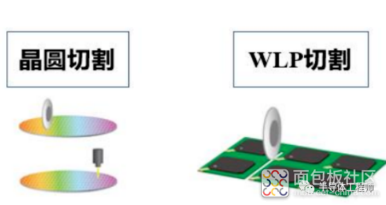
The semiconductor wafer dicing machine divides the wafer containing many chips into wafer particles. The quality and efficiency of cutting directly affect the quality and production cost of chips. Semiconductor wafer dicing machine mainly includes grinding wheel dicing machine and laser dicing machine. Grinding wheel dicing machine is a precision CNC equipment that integrates technologies such as water, gas, electricity, air static pressure high-speed spindle, precision mechanical transmission, sensors and automatic control. It is characterized by low cutting cost and high efficiency, and is suitable for cutting thicker wafers. The laser dicing machine uses a high-energy laser beam to irradiate the surface of the workpiece, so that the irradiated area is partially melted and vaporized, so as to achieve the purpose of dicing.
2. Slicing process
1. Process comparison
Blade cutting methods include one-shot cutting and step-by-step continuous cutting. High efficiency, low cost and long service life. It is the most widely used dicing process and has advantages on thicker wafers (>100 microns). Laser cutting has high precision and high speed. It is mainly suitable for cutting thinner wafers (< 100 microns). When cutting thicker wafers, there is a problem of high temperature damage to the wafer, requiring a blade for secondary cutting. In addition, the laser head is expensive and has a short service life. At present, blade cutting accounts for 80% of the market share, and laser cutting only accounts for 20%. Blade cutting is expected to remain mainstream for a long time.

2. Mainstream technology
Diamond cutting is the mainstream technology for cutting. The cutting uses a blade composed of diamond particles and a binder. During the cutting process, the diamond particles are fixed on the tool body with metallic nickel as abrasive particles. The blade rotates and feeds at a certain speed and uses water as the cutting fluid. During the cutting process, the diamond particles expand and form structures called "chip pockets" with the binder, which scoop through the channel material and then separate it. During the cutting process, the diamond particles are constantly worn away, exposing new particles, keeping the blade sharp and removing cutting debris. Debris generated during cutting will adhere to the blade, so try to prevent the cutting debris from sticking during the cutting process, and handle the cutting debris properly to ensure the normal operation of the blade during the cutting process.
For diamond cutting, the larger the diamond particles, the stronger the cutting ability of the blade, the slower the wear of the diamond particles, and the longer the service life of the blade. However, the larger the particles, the greater the impact of the cutting process on the cutting surface, and it is easy to cause serious defects such as cracks and edge chipping. Smaller diamond grit reduces the impact on the cut surface during cutting and reduces the risk of larger cut defects. However, if the diamond cannot be detached and renewed in time, it is easy to wrap the tool, resulting in a sharp drop in the cutting ability of the blade and serious defects.
The diamond particle concentration of the cutter body will significantly affect the quality of the cutting chips. When the concentration of diamond particles is large, the diamond particles will fall off and be renewed in time with the wear of the binder, which is beneficial to prolong the service life of the blade. Also, the softer the binder, the easier it is for the diamonds to come off, and vice versa. Therefore, cutting with harder binders can cause severe damage to the cut surface, while softer binders have less impact and less damage. The choice of diamond size and concentration should be combined with the type of binder and should be considered comprehensively.
3. Cutting and dicing process
Chips are diced from wafers into individual particles, which are then packaged and ready for use. When dicing, the movement speed of the dicing blade and the rotation speed of the dicing blade should be controlled. The thickness of different chips and the viscosity of the blue film need to have corresponding matching parameters to reduce the phenomenon of debris during the dicing process. Residual silicon slag during cutting can damage cutting tools and chips, resulting in yield loss. During the cutting process, it is necessary to wash with clean water to remove silicon slag, and to control the spray angle and water volume.
Diamond blades cut wafer blocks at high speeds of 30,000-40,000 revolutions per minute. At the same time, the worktable carrying the wafer moves linearly at a certain speed along the tangential direction of the contact point between the blade and the wafer, and the silicon wafers produced by cutting the wafer are washed away by the separator water. To achieve special chip surface protection during dicing, some chips need to be cut twice in all cuts. At this point, the blade for the first cut is relatively wide, and the blade for the second cut is relatively narrow.
4. Factors affecting cutting quality
There are many factors that affect the quality of wafer cutting, including materials, cutting instruments, working environment, cutting methods and other factors. From a material point of view, the silicon substrate and circuit layer materials of a silicon wafer lead to different mechanical properties during the silicon wafer dicing process. The choice of blades of different materials will have different requirements on the cutting method, so it will show different cutting quality. From the point of view of cutting instruments, the choice of cutting table will also affect the cutting quality due to the different cutting power of different machines. From the working environment, the pressure and flow of cooling water are the factors that affect the cutting quality. If the water flow is too slow, the cooling effect will be insufficient, and the heat generated by the cutting friction will be difficult to discharge and accumulate in time, which may cause the diamond abrasive grains to break, reduce the cutting ability and cutting accuracy of the blade, and affect the cutting of the blade because the cutting debris cannot be removed in time. ability. From the perspective of cutting method, it mainly involves cutting depth, blade speed and feed speed. Appropriate parameters are very important to obtain good cutting quality. Other factors, such as machine operator skills, can also affect wafer dicing quality.

5. Cutting defects
The types of defects that are prone to wafer dicing are mainly cracks, chipping and spalling. These defects may cause direct damage to the chip, and may also affect the subsequent packaging and subsequent use reliability of the chip. For example, micro-cracks generated by dicing can introduce stress into the chip and become potentially vulnerable areas of the chip, affecting reliability after packaging. During the cutting process, the chip is impacted by a strong cutter body, and the metal layer and the silicon substrate fall off. If the edge collapse is too large, the functional area of the chip will be damaged, which will directly lead to the failure of the chip. The delamination of the metal layer caused by the impact during the cutting process, although the silicon substrate is not damaged, usually does not cause damage to the function of the chip, but if the peeling area is large and extends to the functional area, it is also very dangerous.